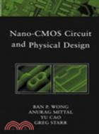
Nano-Cmos Circuit And Physical Design
商品資訊
定價
:NT$ 9088 元優惠價
:90 折 8179 元
若需訂購本書,請電洽客服 02-25006600[分機130、131]。
相關商品
商品簡介
作者簡介
目次
商品簡介
Based on the authors' expansive collection of notes taken over the years, Nano-CMOS Circuit and Physical Design bridges the gap between physical and circuit design and fabrication processing, manufacturability, and yield. This innovative book covers: process technology, including sub-wavelength optical lithography; impact of process scaling on circuit and physical implementation and low power with leaky transistors; and DFM, yield, and the impact of physical implementation.
作者簡介
BAN P. WONG, IENG MIEE, served for five years as a member of the technical program committee of IEEE International Solid-State Circuits Conference and as session chair, cochair, and organizer of a panel session. He has three issued patents. He has led circuit design teams in developing methodology and implementation of high-performance and low-power microprocessors. He is currently Senior Engineering Manager for NVIDIA Corporation.
ANURAG MITTAL received his PhD in applied physics from Yale University. He has codeveloped novel embedded NVM microcontroller and microprocessor solutions including the world’s first truly CMOS-compatible Flash technology. He is Senior Staff Engineer for Virage Logic, Inc.
YU CAO received his PhD in electrical engineering from University of California, Berkeley. He is a postdoctoral researcher in the Berkeley Wireless Research Center. He received the 2000 Beatrice Winner Award at the IEEE International Solid-State Circuits Conference.
GREG STARR received his PhD in electrical engineering from Arizona State University. Currently, he is a Senior Design Manager at Xilinx Corporation.
目次
FOREWORD.
PREFACE.
1 NANO-CMOS SCALING PROBLEMS AND IMPLICATIONS.
1.1 Design Methodology in the Nano-CMOS Era.
1.2 Innovations Needed to Continue Performance Scaling.
1.3 Overview of Sub-100-nm Scaling Challenges and Subwavelength Optical Lithography.
1.4 Process Control and Reliability.
1.5 Lithographic Issues and Mask Data Explosion.
1.6 New Breed of Circuit and Physical Design Engineers.
1.7 Modeling Challenges.
1.8 Need for Design Methodology Changes.
1.9 Summary.
References.
PART I: PROCESS TECHNOLOGY AND SUBWAVELENGTH OPTICAL LITHOGRAPHY: PHYSICS, THEORY OF OPERATION, ISSUES, AND SOLUTIONS.
2 CMOS DEVICE AND PROCESS TECHNOLOGY.
2.1 Equipment Requirements for Front-End Processing.
2.2 Front-End-Device Problems in CMOS Scaling.
2.3 Back-End-of-Line Technology.
References.
3 THEORY AND PRACTICALITIES OF SUBWAVELENGTH OPTICAL LITHOGRAPHY.
3.1 Introduction and Simple Imaging Theory.
3.2 Challenges for the 100-nm Node.
3.3 Resolution Enhancement Techniques: Physics.
3.4 Physical Design Style Impact on RET and OPC Complexity.
3.5 The Road Ahead: Future Lithographic Technologies.
References.
PART II: PROCESS SCALING IMPACT ON DESIGN 4 MIXED-SIGNAL CIRCUIT DESIGN.
4.1 Introduction.
4.2 Design Considerations.
4.3 Device Modeling.
4.4 Passive Components.
4.5 Design Methodology.
4.6 Low-Voltage Techniques.
4.7 Design Procedures.
4.8 Electrostatic Discharge Protection.
4.9 Noise Isolation.
4.10 Decoupling.
4.11 Power Busing.
4.12 Integration Problems.
4.13 Summary.
References.
5 ELECTROSTATIC DISCHARGE PROTECTION DESIGN.
5.1 Introduction.
5.2 ESD Standards and Models.
5.3 ESD Protection Design.
5.4 Low-C ESD Protection Design for High-Speed I/O.
5.5 ESD Protection Design for Mixed-Voltage I/O.
5.6 SCR Devices for ESD Protection.
5.7 Summary.
References.
6 INPUT/OUTPUT DESIGN.
6.1 Introduction.
6.2 I/O Standards.
6.3 Signal Transfer.
6.4 ESD Protection.
6.5 I/O Switching Noise.
6.6 Termination.
6.7 Impedance Matching.
6.8 Preemphasis.
6.9 Equalization.
6.10 Conclusion.
References.
7 DRAM.
7.1 Introduction.
7.2 DRAM Basics.
7.3 Scaling the Capacitor.
7.4 Scaling the Array Transistor.
7.5 Scaling the Sense Amplifier.
7.6 Summary.
References.
8 SIGNAL INTEGRITY PROBLEMS IN ON-CHIP INTERCONNECTS.
8.1 Introduction.
8.2 Interconnect Parasitics Extraction.
8.3 Signal Integrity Analysis.
8.4 Design Solutions for Signal Integrity.
8.5 Summary.
References.
9 ULTRALOW POWER CIRCUIT DESIGN.
9.1 Introduction.
9.2 Design-Time Low-Power Techniques.
9.3 Run-Time Low-Power Techniques.
9.4 Technology Innovations for Low-Power Design.
9.5 Perspectives for Future Ultralow-Power Design.
References.
PART III: IMPACT OF PHYSICAL DESIGN ON MANUFACTURING/YIELD AND PERFORMANCE.
10 DESIGN FOR MANUFACTURABILITY.
10.1 Introduction.
10.2 Comparison of Optimal and Suboptimal Layouts.
10.3 Global Route DFM.
10.4 Analog DFM.
10.5 Some Rules of Thumb.
10.6 Summary.
References.
11 DESIGN FOR VARIABILITY.
11.1 Impact of Variations on Future Design.
11.2 Strategies to Mitigate Impact Due to Variations.
11.3 Corner Modeling Methodology for Nano-CMOS Processes.
11.4 New Features of the BSIM4 Model.
11.5 Summary.
References.
INDEX.
主題書展
更多
主題書展
更多書展本週66折
您曾經瀏覽過的商品
購物須知
外文書商品之書封,為出版社提供之樣本。實際出貨商品,以出版社所提供之現有版本為主。部份書籍,因出版社供應狀況特殊,匯率將依實際狀況做調整。
無庫存之商品,在您完成訂單程序之後,將以空運的方式為你下單調貨。為了縮短等待的時間,建議您將外文書與其他商品分開下單,以獲得最快的取貨速度,平均調貨時間為1~2個月。
為了保護您的權益,「三民網路書店」提供會員七日商品鑑賞期(收到商品為起始日)。
若要辦理退貨,請在商品鑑賞期內寄回,且商品必須是全新狀態與完整包裝(商品、附件、發票、隨貨贈品等)否則恕不接受退貨。


