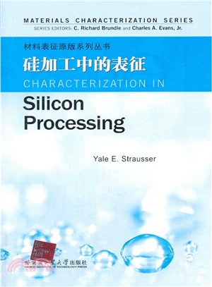
矽加工中的表徵(簡體書)
商品資訊
相關商品
商品簡介
名人/編輯推薦
目次
書摘/試閱
商品簡介
《硅加工中的表征》是材料表征原版系列叢書之一。全書共分六章,內容包括:材料表征技術在硅外延生長中的應用;多晶硅導體;硅化物;鋁和銅基導線;級鎢基導體;阻隔性薄膜。本書適合作為相關領域的教學、研究、技術人員以及研究生和高年級本科生的參考書。
名人/編輯推薦
《硅加工中的表征(英文)》由哈爾濱工業大學出版社出版。
目次
Preface to the Reissue of the Materials Characterization Series ix
Preface to Series x
Preface to the Reissue of Characterization in Silicon Processing xi
Preface xii
Contributors xiv
APPLICATION OF MATERIALS CHARACTERIZATION TECHNIQUES TO SILICON EPITAXIAL GROWTH
1.1 Introduction 1
1.2 Silicon Epitaxial Growth 2
Basic Chemical Reactions 2, Precleaning Considerations 3,
Reactor Types 3
1.3 Film and Process Characterization 4
Crystal Quality 4, PrecleanQuality 6, Thickness 9, Dopant
Concentration and Dopant Profiling 12
1.4 Selective Growth 14
Basic Process Considerations 14, Defect Density and Growth
Morphology 15, Predean Quality 18, Thickness 18
1.5 Si1 _xGex Epitaxial Growth 18
Material Considerations 18, Reactor Types 19
1.6 Si1_ xGex Material Characterization 20
Composition and Thickness 20, Growth Morphology 22, Lattice
Strain and Critical Thickness 23, Relaxation Kinetics 24, Bandgap
Measurements 24, Interracial Abruptness and Outdiffusion 25,
Impurity Profiles 25
1.7 Summary 26
POLYSILICON CONDUCTORS
SILICIDES
ALUMINUM— AND COPPER—BASED CONDUCTORS
TUNGSTEN—BASED CONDUCTORS
BARRIER FILMS
APPENDIX: TECHNIQUE SUMMARIES
書摘/試閱
Although it is much more a function of etch parameter variations than ofpolysiliconmaterials properties, another problem which frequently arises is that of variations inthe cross-sectional profile of the etched potysilicon lines. The standard procedure formonitoring this problem is to prepare samples destructively by cleaving etched wafersperpendicular to the poly lines, coating the samples, and then evaluating them in crosssection in an SEM. The time and wasted material in this process can be significantlyreduced by using LS, which has been shown to produce signatures that are extremelysensitive to dimensions and angles in periodic fields of etched structures. This technique requires only the momentary reflection of a light beam from the area of interestto produce a signature which can be compared to that of a properly etched area.
2.5 Subsequent Processing
During most of the subsequent processing steps that polysilicon layers may see, theonly process input which produces any change is the time-temperature product whichresults in grain growth and dopant diffusion effects. The two exceptions are thedeposition, anneal, and oxidation steps involved in the formation of polycide (metalsilicide on polysilicon) structures and the dielectric encapsulation of the polysilicon.
Polycides
The polycide formation process will be illustrated with the example of a tungsten-polycide system. Various other metal-silicide systems are used, but many of thematerials-related problems are similar. The silicide film is formed either by the deposition of a pure metal film and an anneal to form the silicide layer or by direct deposition of the metal silicide onto the polysilicon. In the tungsten-polycide case, it isusually done through the CVD ofWSi2.2. (The excess silicon will be depleted duringa subsequent oxidation step.) Two important materials issues in this step are that thepolysilicon surface must be clean so that the silicide layer will adhere to it and thatthe deposition system must have a low background pressure so that tungsten oxidesare not formed during deposition. The glaze discussed previously, which is formedduring some types of doping, must be removed, as must any other contaminantspicked up after polysilicon deposition. For the level of surface contamination controlrequired here, AES is typically the best tool to check cleanliness. Volume contamina-tion in the deposited silicide, principally oxygen, picked up from poor depositionsystem base pressures may also be found by AES, although post-deposition profilingby dynamic SIMS may be required to see the very low levels of oxygen which canbegin to form tungsten oxides. Monitoring the Si/W ratio, which can be of concern,is best done by RBS, since differential sputtering effects between the tungsten andthe silicon make all sputter-profiling techniques problematic.
主題書展
更多
主題書展
更多書展本週66折
您曾經瀏覽過的商品
購物須知
大陸出版品因裝訂品質及貨運條件與台灣出版品落差甚大,除封面破損、內頁脫落等較嚴重的狀態,其餘商品將正常出貨。
特別提醒:部分書籍附贈之內容(如音頻mp3或影片dvd等)已無實體光碟提供,需以QR CODE 連結至當地網站註冊“並通過驗證程序”,方可下載使用。
無現貨庫存之簡體書,將向海外調貨:
海外有庫存之書籍,等候約45個工作天;
海外無庫存之書籍,平均作業時間約60個工作天,然不保證確定可調到貨,尚請見諒。
為了保護您的權益,「三民網路書店」提供會員七日商品鑑賞期(收到商品為起始日)。
若要辦理退貨,請在商品鑑賞期內寄回,且商品必須是全新狀態與完整包裝(商品、附件、發票、隨貨贈品等)否則恕不接受退貨。


