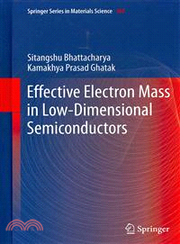
Effective Electron Mass in Low-Dimensional Semiconductors
商品資訊
ISBN13:9783642312472
替代書名:Effective Electron Mass in Low-Dimensional Semiconductors
出版社:Springer Verlag
作者:Sitangshu Bhattacharya; Kamakhya Prasad Ghatak
出版日:2012/10/28
裝訂/頁數:精裝/400頁
定價
:NT$ 12759 元若需訂購本書,請電洽客服 02-25006600[分機130、131]。
商品簡介
作者簡介
相關商品
商品簡介
This book deals with the Effective Electron Mass (EEM) in low dimensional semiconductors. The materials considered are quantum confined non-linear optical, III-V, II-VI, GaP, Ge, PtSb2, zero-gap, stressed, Bismuth, carbon nanotubes, GaSb, IV-VI, Te, II-V, Bi2Te3, Sb, III-V, II-VI, IV-VI semiconductors and quantized III-V, II-VI, IV-VI and HgTe/CdTe superlattices with graded interfaces and effective mass superlattices. The presence of intense electric field and the light waves change the band structure of optoelectronic semiconductors in fundamental ways, which have also been incorporated in the study of the EEM in quantized structures of optoelectronic compounds that control the studies of the quantum effect devices under strong fields. The importance of measurement of band gap in optoelectronic materials under strong electric field and external photo excitation has also been discussed in this context. The influence of crossed electric and quantizing magnetic fields on the EEM and the EEM in heavily doped semiconductors and their nanostructures is discussed. This book contains 200 open research problems which form the integral part of the text and are useful for both Ph. D aspirants and researchers in the fields of solid-state sciences, materials science, nanoscience and technology and allied fields in addition to the graduate courses in modern semiconductor nanostructures. The book is written for post graduate students, researchers and engineers, professionals in the fields of solid state sciences, materials science, nanoscience and technology, nanostructured materials and condensed matter physics.
作者簡介
Dr. S. Bhattacharya obtained his M. Sc. and Ph.D Degree from Electronic Science of the University of Calcutta and Jadavpur University, India in 2003 and 2009 respectively and is presently working at the Centre for Electronics Design and Technology, Indian Institute of Science, Bangalore. His current work involves the investigations of transport properties of different nanoscaled materials and devices under various external conditions. He is the co-author of more than 50 scientific research papers in different aspects of nanostructures in international peer-reviewed journals of high repute. He is also the co-author of the FOUR research monographs entitled "Einstein Relation in Compound Semiconductors and Their Nanostructures" Springer Series in Materials Science, Vol. 116,2009 which is the first book on Einstein relation and contains more than 100 open research problems, "Photoemission from Optoelectronic materials and their nanostructures",Springer Series in Nano structure Science and Technology, USA in 2009 as the first book solely devoted to Photoemission from nanostructured optoelectronic materials and contents more than 100 open research problems, "Thermo electric power in nano structured materials under strong magnetic field" Springer Series in Materials Science Vol. 137 ,2010 and contents one hundred and fifty open research problems and "Fowler-Nordheim Field Emission from Semiconductor Nanostructures" Springer Series in Solid State Sciences, Vol. 170, 2011 which is the first book on Fowler-Nordheim Field Emission containing 200 open research problems respectively. His present research interests are the quantum effect devices and nonlinearities. Besides, he is an invited speaker in different reputed International Conferences on nanoscale systems and devices. Born in India in 1953.Professor K. P. Ghatak obtained his B.E degree in Electronics and Telecommunication Engineering in 1974 from the then Bengal Engineering college Shibpur(Presently Bengal Engineering and Science University) in 1974, M.Tech and PhD(Tech) degrees from the Institute of Radio Physics and Electronics of The University of Calcutta in 1976 and 1988 respectively.He joined as Lecturer in the Institute of Radio Physics and Electronics of the University of Calcutta in 1983, Reader in the Department of Electronics and Telecommunication of Jadavpur University in 1987 and Professor in the Department of Electronic Science of the University of Calcutta in 1994 and was at the top of the merit list in all the cases respectively. Professor K. P. Ghatak is the First Recipient of the Degree of Doctor of Engineering of Jadavpur University in 1991 since the University inception in 1955 and in the same year he received the Indian National Science Academy visiting fellowship to IIT-Kharagpur. His present research interests are nano science and number thoery. He is the principal co-author of more than 200 research papers on Semiconductor and Nanoscience in eminent peer-reviewed International Journals and more than 50 research papers in the Proceedings of the International Conferences held in USA and many of his papers are being cited many times. Professor Ghatak is the invited Speaker of SPIE, MRS, etc. and is the referee of different eminent Journals. He is the supervisor of more than two dozens of Ph.D candidates in various aspects of materials and nanoscience and many of them are working as Professor, Associate Professor and Assistant Professor in different Universities and reputed Academic Institutions. He is the principal co-author of the said FOUR research monographs. The All Indian Council For Technical Education has selected the first Research and Development project in his life for the best project award in Electronics and second best research project award considering all the branches of Engineering for the year 2006.
主題書展
更多
主題書展
更多書展今日66折
您曾經瀏覽過的商品
購物須知
外文書商品之書封,為出版社提供之樣本。實際出貨商品,以出版社所提供之現有版本為主。部份書籍,因出版社供應狀況特殊,匯率將依實際狀況做調整。
無庫存之商品,在您完成訂單程序之後,將以空運的方式為你下單調貨。為了縮短等待的時間,建議您將外文書與其他商品分開下單,以獲得最快的取貨速度,平均調貨時間為1~2個月。
為了保護您的權益,「三民網路書店」提供會員七日商品鑑賞期(收到商品為起始日)。
若要辦理退貨,請在商品鑑賞期內寄回,且商品必須是全新狀態與完整包裝(商品、附件、發票、隨貨贈品等)否則恕不接受退貨。


